
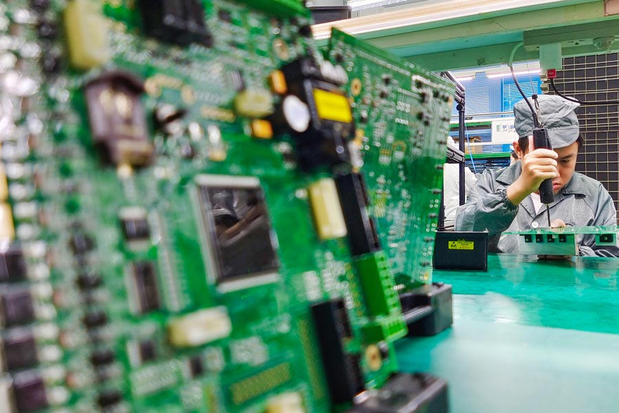
To ensure the finished product’s performance, the printed circuit board (PCB) manufacturing process involves a rigorous procedure. Though circuit boards can be single, double, or multilayered, the fabrication methods differ only after the first layer is created. Because of differences in PCB structure, some may require 20 or more steps during industrial production.
The sequence required to manufacture printed circuit boards is proportional to their complexity. Any skipped or shortened step may harm the circuit board’s performance. However, the PCBs should function properly as critical electrical parts once finished.
A PCB is made up of four major components:
- Substrate: The first and most process is the substrate, which is typically made of fibreglass. Fibreglass is because it gives the PCB core strength and helps it resist breakage. Consider the substrate to be the “skeleton” of the PCB.
- Copper Layer: This layer can be copper foil or a full-on copper topcoat, depending on the type of board. Whatever method is used, the purpose of the copper remains the same: to carry electrical impulses to and from the PCB, much like your stress response does between your brain and your muscles.
- Solder Mask: The third component of the PCB is the solder mask, a polymer layer that helps protect the copper from short-circuiting when it comes into interaction with the atmosphere. As a result, the solder concealer serves as the PCB’s “skin.”
- Silkscreen: The silkscreen is the final part of the circuit board. The silkscreen is generally located on the board’s component side and displays replacement parts, logos, symbols, switch settings, element references, and test points. The silkscreen is also referred to as legend or nomenclature.
PCB design, both digital and physical
Every custom PCB design results from a customer’s particular needs in the electronic industry. Using special software, the designers design the PCB based on their specifications. The result of their layout is a blueprint of the custom PCB, which should include all necessary PCB specifications for makers to proceed with PCB manufacturing.
To avoid problems during the production stage, designers should consult with manufacturers about software applications before PCB design. Discrepancies caused by the designer’s software calling incorrect sequences in Gerber file generation can cause problems. Although specific software encodes all technical specifications about the PCB, such as copper tracking layers, drill drawings, apertures, and component terminology, the data transferred into manufacturer software may differ from the predecessor. As a result, special care must be taken during PCB design to avoid repeating the creative process multiple times.
China PCB is a professional PCB (printed circuit board) manufacturer that offers PCB design, manufacturing, and fitted models to a diverse range of companies in the desktop, industrial, RF products, automobiles, securities, telecommunication services, and other electronic equipment markets.
As a full-service turnkey provider of custom electronics, China PCB can help with everything from design and prototype testing to new product introduction and full-rate production.
To remain competitive, China PCB is your one-stop-shop for PCB manufacturing, component procurement, arrangement, and turnkey jobs, or select any choices that best suit your needs.
ChinaPCBOne Technology LTD. is the author of this article on PCB manufacturing. Find more information, about PCB manufacturer.